From the engineering desk
The DFM Checklist: 20 Decisions to Make Before Tooling
A mold problem caught after the first trial costs $5K–$50K and weeks of delay. The 20 design-for-manufacturability decisions that catch it for free instead.
By Axon Labs Engineering
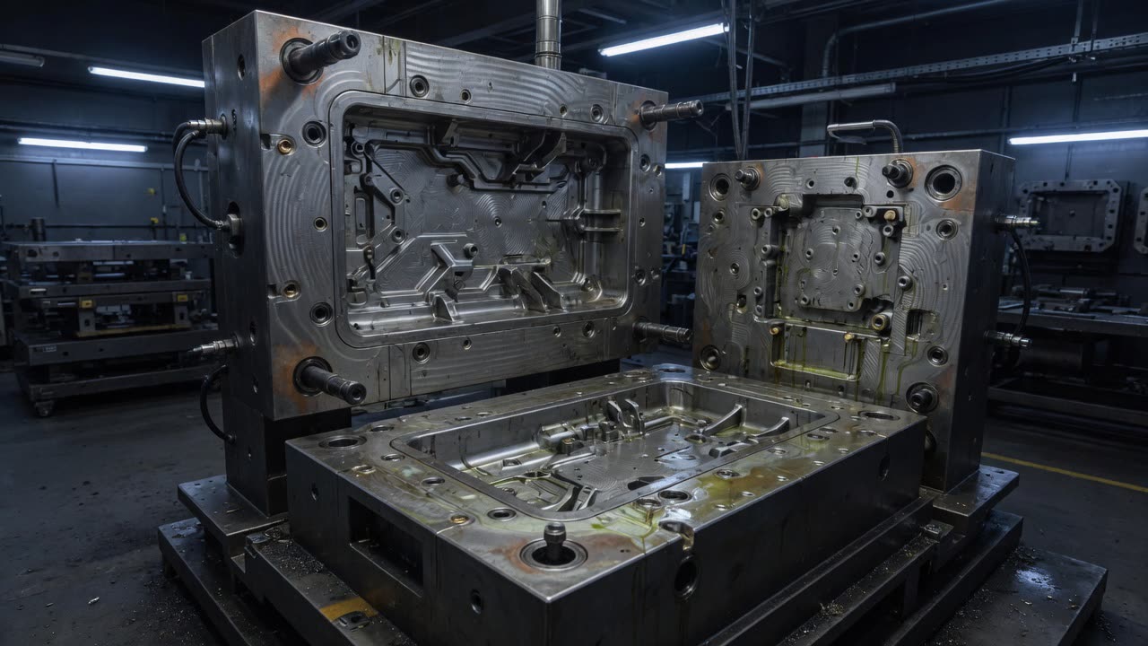
If a mold problem only surfaces after the first injection trial, it typically costs $5,000 to $50,000 and pushes the schedule back weeks — a bill a 30-minute design review could have avoided entirely. The same math holds on the board: 2026 data puts the average PCB respin at $28,500 and 16 days, and a single wrong footprint is enough to trigger one. Design for manufacturability isn't a phase. It's twenty specific decisions, and this is the checklist we run before any tool gets cut.
Key takeaways
- A DFM issue caught after the first mold trial costs $5,000–$50,000 and weeks of delay; the same check at design review costs a 30-minute meeting.
- In 2026, PCB projects average 2.9 respins at $28,500 and 16 days each — and incorrect footprints alone are a leading single cause.
- Parting-line placement, draft angle and wall-thickness ratios must be locked before tooling starts — changing any of them after steel is cut is one of the most expensive mistakes in hardware.
Why does DFM matter more than the design itself?
What does a missed DFM issue actually cost?
The enclosure and molding checklist (10 decisions)
- Draft angle, everywhere. 1–2° per side is the working rule of thumb, with a 2° minimum on most surfaces; light texture needs 3°, heavy texture 5° or more (Protolabs). A wall with zero draft either won't eject or will drag and scar on the way out.
- Wall thickness, held constant. Vary it and you invite sink marks and warping as the thick sections cool slower than the thin ones.
- Rib thickness at 50–60% of nominal wall. Full-thickness ribs telegraph as visible sink marks on the opposite face.
- Rib and boss draft, 0.5–1.0° per side — smaller than the main wall draft, but still non-zero.
- Parting line agreed at design review, not after tooling starts. Moving it once a mold exists is one of the most expensive changes in the entire program.
- Gate location chosen for flow, not convenience. A poorly placed gate creates weld lines exactly where cosmetic surfaces or structural loads can't tolerate them.
- Undercuts minimized or engineered with a clear release mechanism. Every undercut is a slide, a lifter, or a redesign — decide which, on purpose.
- Snap-fits sized for real material fatigue, not just first-assembly feel. A snap that works once in the demo and cracks on the tenth field disassembly is a returns problem, not a tooling one.
- PCBA height and connector alignment checked against the enclosure, not assumed. Battery installation, LED visibility, button feel and cable bend radius all live at this boundary and are cheap to fix in CAD, expensive to fix in steel.
- Screw posts and sealing surfaces sized for the actual fastener and gasket, not a placeholder. Heat paths belong on this list too — thermal problems discovered after tooling means redesigning around a mold that already exists.
The PCB and assembly checklist (10 decisions)
- Every footprint verified against the actual component datasheet. Incorrect footprints are among the single most common causes of prototype failure — one wrong footprint can force a full respin.
- Design rules matched to your fabricator's real capabilities, not generic defaults — trace width, spacing and via specs that your board house can actually produce at yield, referenced against standards like IPC-2221C and IPC-2152.
- DFM checks run iteratively through the design stages, not as a single gate at the end — catching an error at 60% layout is cheaper than catching it at 100%.
- Test points placed for factory test access, not just debug convenience — the fixture that validates every unit off the line depends on them.
- Thermal relief and copper pour reviewed for both manufacturability and function — a pour that's hard to solder is a yield problem hiding as a design choice.
- Component placement checked for pick-and-place and reflow reality — tall components near short ones can create shadowing and uneven reflow.
- Panelization planned before layout is finalized, not bolted on afterward — break-away tabs and fiducials belong in the original design.
- Silkscreen and polarity markings verified legible at production scale — a mark that's clear at 400% zoom in CAD can vanish at 1:1 on the actual board.
- Connector and mounting-hole tolerances stack-checked against the enclosure — the PCB and the case are one tolerance chain, not two independent drawings.
- A named DFM reviewer signs off before Gerbers or tooling release — accountability, not just a checklist, is what actually catches the error before it becomes a $28,500 respin.
When should DFM review actually happen?
| Review point | What it catches | Cost if skipped |
|---|---|---|
| Concept freeze | Fundamental moldability, gross tolerance conflicts | Architecture rework — days, not weeks |
| Design review, pre-tooling | Draft, wall thickness, parting line, footprints, DRC violations | $5K–$50K tool rework, or a full PCB respin |
| Pre-release, final CAD | Last-minute edits that broke an earlier fix | A second respin on top of the first |
A factory can't build your intentions. It builds exactly what the drawing says — including the mistakes.
The bottom line
- A DFM issue caught in design review costs a meeting. The same issue caught after tooling starts costs $5K–$50K on the enclosure side, or a $28.5K, 16-day respin on the board.
- The checklist is specific, not aspirational: draft angle, wall thickness, parting line, footprint verification and a named sign-off — twenty decisions, not a vibe.
- Run DFM review at three points, not one — concept freeze, pre-tooling design review, and final pre-release verification. The middle pass is the one teams skip, and the one that matters most.
Frequently asked questions
What is DFM in hardware product development?
How much does a missed DFM issue cost?
What is the correct draft angle for injection molding?
When should a DFM review happen in the development process?
What causes most PCB respins?
Sources
- RJC Mold — Design for Manufacturability (DFM) in Injection Molding · verified 31 July 2026
- Crescent Industries — DFM Guide for Injection Molding: Best Practices for Design & Manufacturing · verified 31 July 2026
- SILKBRIDGE — What Is DFM for Injection Molding? A Plastic Part Design Guide Before Tooling · verified 31 July 2026
- Sierra Circuits — DFM Issues to Check Before PCB Manufacturing · verified 31 July 2026
- Sierra Assembly — Design for Manufacturing (DFM) in PCB Assembly: Best Practices for 2026 · verified 31 July 2026
- Protolabs — Draft Angle Guidelines for Injection Molding · verified 31 July 2026
- Comtec Labs — PCB Design for Manufacturing Checklist: A European Engineer's Guide · verified 31 July 2026
- CADSTROM — The Hidden Cost of PCB Respins: Why 90% of First Prototypes Fail · verified 31 July 2026
- JLCPCB — Top DFM and DFA Rules That Ensure PCB Assembly Success · verified 31 July 2026
If the product has to ship, talk to the team that builds for that outcome.
Senior engineer on the first call. NDA before technical detail. References available under NDA after qualification. Or start with a fixed-fee feasibility study.