From the engineering desk
How Much Does It Cost to Develop a Hardware Product in 2026?
The line-by-line answer: $75K–$400K+ from concept to market, where every dollar goes, the multiplier nobody budgets, and a worksheet to plan with.
By Axon Labs Engineering
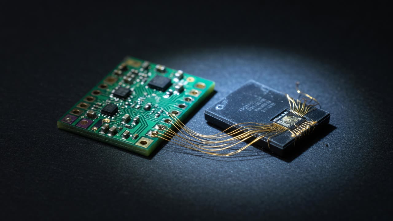
In 2026, taking a hardware product from concept to market-ready typically costs $75,000 to $400,000 and beyond, per Calcix’s Hardware Product Development Budgeting Guide — and roughly 70% of it goes to engineering labor and tooling. Those are the headline numbers. This article is about the layer beneath them: what each line item actually costs, which phase consumes it, why programs blow through estimates that looked conservative, and the planning worksheet we use with clients before a dollar is committed.
Key takeaways
- Plan $75K–$125K for simple products, $125K–$250K for connected consumer devices, and $250K–$400K+ where regulation enters (Calcix, 2026) — engineering labor plus tooling consume ~70% of the total.
- The big line items in 2026: electronics & PCB $15K–$75K, mechanical $10K–$60K, prototyping $15K–$150K across 3–5 rounds, tooling $15K–$100K per mold, certification $10K–$50K (Integra Sources; Calcix).
- The real budget killer is iteration count, not rates: each full prototype spin costs 6–10 weeks. Hold a 25% contingency and spend feasibility money to kill doomed architectures on paper.
What does hardware development cost in 2026?
The line items, one by one
- Industrial design — from $10K. Form exploration, CMF, ergonomics. Cheap relative to what it prevents: an enclosure that fights the antenna or the mold.
- Electronics & PCB — $15K–$75K. Architecture, schematic, layout, component engineering, EMC preparation (Integra Sources, 2026). Radios and power management sit at the top of the range.
- Firmware & software — commonly 2–4× the hardware design cost. The ratio surprises founders every time (ByteSnap); testing and debugging on real hardware is where the hours live. System integration adds $5K–$25K.
- Mechanical engineering — $10K–$60K. Enclosures, stack-ups, thermal paths, DFM geometry.
- Prototyping — $15K–$150K across the program. Not one build: 3–5 full rounds at rising fidelity (Calcix, 2026).
- Tooling — $15K–$100K per mold. Aluminum prototype molds start near $1K–$10K; hardened production steel runs $50K–$200K+ (RapidDirect). Count your molds — a two-shell product with buttons is rarely one.
- Certification — $10K–$50K, or 10–15% of budget. FCC testing runs $3K–$5K for basic devices and $9K–$15K with Bluetooth/Wi-Fi (Compliance Testing); CE spans self-declaration to $20K+ with a notified body; medical multiplies it.
Where the money lands, phase by phase
| Phase | You’re paying for | Cost character |
|---|---|---|
| Discovery & feasibility | Architecture, risk register, cost model | Small, fixed — and it prices everything after it |
| Proof of concept | The riskiest assumptions, tested in hardware | Contained; kills bad paths at demo cost |
| EVT — engineering validation | Real components, first integrated boards | Prototype spins begin consuming budget |
| DVT — design validation | Near-final units, pre-cert testing | Peak engineering burn; certification queues start |
| PVT — production validation | Tooling, fixtures, factory bring-up | Capital-heavy: steel, test rigs, pilot runs |
The multiplier nobody budgets: iteration count
The lines nobody puts in version one of the budget
- Test engineering. Factory fixtures, firmware test modes, pass/fail criteria. Nobody budgets it the first time; everybody budgets it the second.
- Certification re-queues. A failed EMC pre-scan means a board spin plus a new lab slot — weeks and five figures, at the worst point in the schedule.
- Supply-chain requalification. The part that was in stock for five prototypes needs multi-source availability for fifty thousand units.
- Security and compliance engineering. As of 2026 this is a real line: the EU Cyber Resilience Act’s reporting obligations start 11 September 2026, and CRA-readiness — secure boot, signed updates, SBOM tooling — is dramatically cheaper designed in than retrofitted.
- The pilot run’s scrap. First articles, yield learning, and the units you destroy on purpose. Budget them as tuition.
What actually makes it cheaper
- Buy feasibility before engineering. A few weeks of architecture, risk and cost modeling de-risks every later dollar — it’s the highest-leverage spend in the program.
- Design to cost from day one. BOM ceilings as first-class constraints, right-sized silicon, sensor fusion instead of added sensors — architecture decides 90% of unit cost; purchasing shaves the rest.
- DFM before the first prototype exists. Draft angles, part counts, test points — the cheapest DFM review is the one held before geometry hardens.
- Match the team model to the program. Senior hardware engineers take six-plus months to hire to productivity; a development firm’s rate buys down iteration count on a first product, and iterations — not hourly rates — dominate the total. The full trade-off is in our development guide.
A planning worksheet you can steal
| Phase | Planning range | Main contents |
|---|---|---|
| Discovery & feasibility | $10K–$25K | Architecture, risk register, cost model, cert plan |
| Proof of concept | $20K–$50K | Highest-risk assumptions in working hardware |
| Product engineering (EVT→DVT) | $60K–$120K | Electronics, firmware, mechanical, 3–5 spins |
| Productization & tooling | $25K–$80K | DFM, production files, molds, fixtures |
| Certification | $10K–$30K | Pre-scans, lab queues, documentation |
| Pilot & test engineering | $10K–$25K | Factory bring-up, fixtures, first articles |
| Subtotal | $135K–$330K | Then add the 25% contingency |
Budgets don’t die from line items. They die at spin four.
The bottom line
- Budget $75K–$400K+ by complexity tier; ~70% is engineering labor and tooling, and firmware commonly runs 2–4× the hardware design cost.
- Costs are decided upstream of where they’re paid: architecture sets the tooling bill, layout sets the certification bill, feasibility sets everything.
- Guard the multiplier: 3–5 spins is normal, each spin is 6–10 weeks, and a 25% contingency is the minimum honest buffer.
Frequently asked questions
How much does it cost to develop a hardware product in 2026?
Why does hardware cost so much more than software to develop?
How much does a hardware prototype cost?
How much does product certification cost?
What's the best way to reduce hardware development cost?
Sources
- Calcix — How Much Does it Cost to Build a Hardware Prototype? (2026 Guide) · verified 19 July 2026
- Integra Sources — The Anatomy of a Hardware Project: A Detailed Breakdown of Development Cost · verified 19 July 2026
- ByteSnap — Cost to Design a New Electronic Product · verified 19 July 2026
- Innovative Design Products — Electronics Product Design Budget Planning for Businesses · verified 19 July 2026
- RapidDirect — Injection Molding Cost Breakdown: A 2026 Pricing & DFM Strategy Guide · verified 19 July 2026
- Compliance Testing — How Much Does FCC Testing Cost? · verified 19 July 2026
- Titoma — NRE Meaning in Engineering: What It Costs and Why It Matters · verified 19 July 2026
- NED Labs — Hardware Development Costs: What Nobody Tells You · verified 19 July 2026
- TriMech Design — How Much Does Product Development Cost: Design & Prototype · verified 19 July 2026
- EcoComply — CE Marking Cost for Electronics (2026) · verified 19 July 2026
If the product has to ship, talk to the team that builds for that outcome.
Senior engineer on the first call. NDA before technical detail. References available under NDA after qualification. Or start with a fixed-fee feasibility study.